R&D Field of interest
The University of Cadiz Diamond R&D group is integrated by 20 investigators with: (i) a laboratory of Diamond growth (p- and n-doping machines as well as PVD machines for metals-oxydes-nitrides) and semiconducting materials technology and characterisation. His activity is focused on:

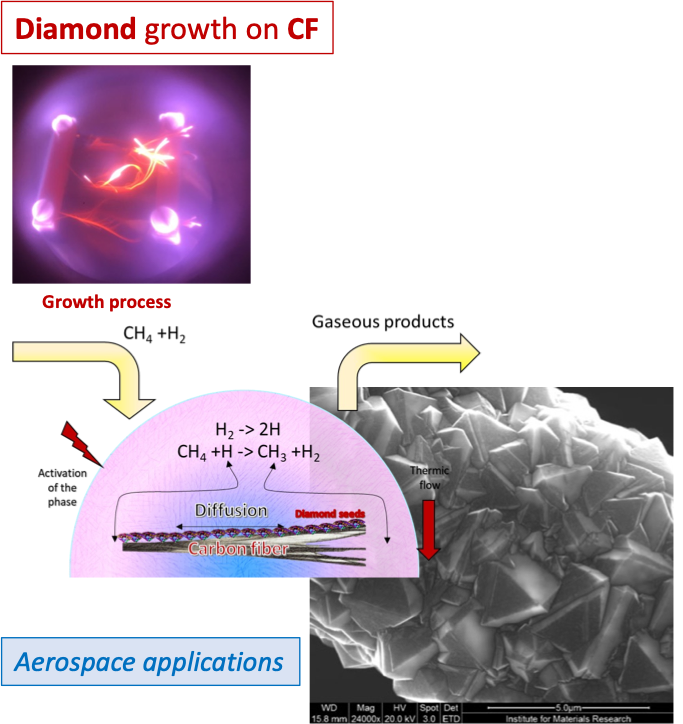
1.- Aerospace Materials: Modification of the CFRP material in order to transform it in:
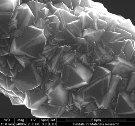
- Electrically and thermically conductive material to avoid damage during lightning impacts, thanks to the diamond (heavily B-doped) growth around the CF.
- Functionalize the CFRP making possible, for example, electronic structurally integrated sensors (nanomembranes for pressure sensors, integrated diodes for T sensors, … or energy harvesting systems using the wing bendings as energy source. Piezoelectric material (grown by PVD at 700ºC), AlNSc, embedded in diamond (grown by MPCVD) around the CF make it possible.
R&D activities:
- Industrial process to deposit diamond on carbon fibre and transform CFRP in electrical and thermal conductive material.
- Micro- and nano-sensors structurally incorporated in the CFRP material.
- Energy harvesting from wing bending through diamond/AlScN/diamond related devices
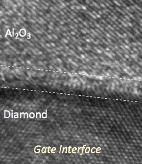
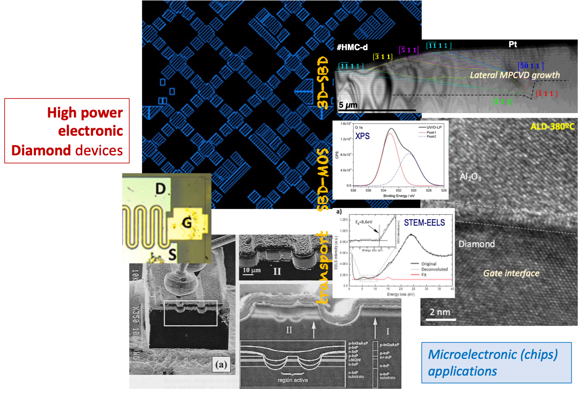
2.- Diamond semiconducting devices for high power electronic: Thanks to the MPCVD machines, n- and p-doped diamond layers are grown in the laboratory following previous designed architectures and followed by electro-lithography and FIB-related steps. MOSFETs, JFETs and SBD (Schottky barrier diodes) oriented to Power Electronic applications have been developed in the laboratory and patented. Devices from µm-scale down to nm-scale are developed for high power application.
R&D activities :
1.Diamond Super-condensers for energy storage: high velocity storage power and high capacity
2.Diamond FET transistors for high power applications: MOSFETs with ZrO2-based gate, JFET, MESFETs, …
3.Diamond junction barrier SBD for very high current applications and high voltages

3.- Diamond nanoparticules for medical aplication: Using colour centers located in the low body absorption part of the IR spectrum, excitation of them through the skin (non-invasive technique) allows to obtain information of organs of the human body as local temperature, …
For the three activities, the laboratory has acquired and installed: (i) PVD (sputtering and e-beam) system working up to 800ºC, (ii) Electro-lithography set-up (spinner, glove-box, FIB-dial beam), (iii) Nano-deposition of metals and dielectric material under ion-beam of a FIB-dual beam, (iv) 2 MPCVD machines for diamond deposition (one for n-doping and the other for p-doping), (v) electrical (I/V, C/V) measurement set-up (prober), (vi) optical characterization as UV-IR PL, Raman, Micro-Raman.


